Factory Audit;
Goods Inspection;
Third Party Test.

WHAT ARE YOU LOOKING FOR?


Detailed Overview of the Photovoltaic Semiconductor Silicon Wafer Manufacturing Process
Jun 28, 2024Silicon wafers are the core material in the photovoltaic semiconductor industry, with a complex manufacturing process and high technical requirements. The basic process for manufacturing silicon wafers is as follows:
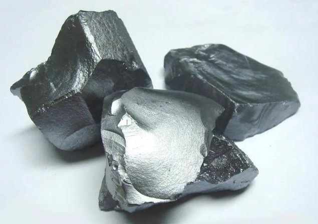
1、Raw Material Preparation The raw material for silicon wafers is high-purity silicon, usually in the form of polycrystalline or monocrystalline silicon. These silicon blocks are typically extracted from ores and then refined and purified to produce high-purity polycrystalline silicon.
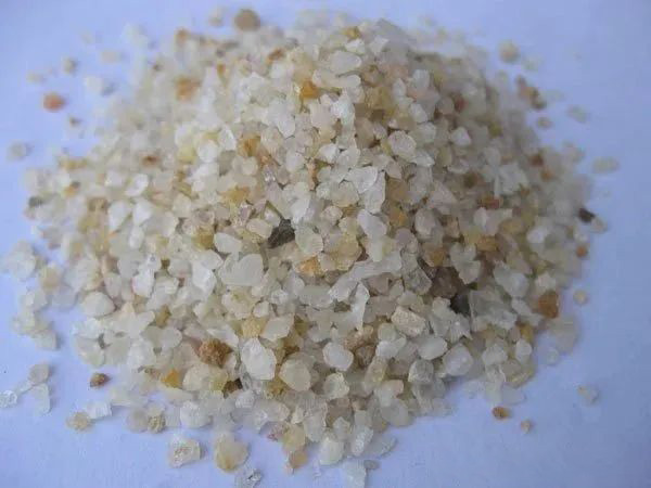
2、Polycrystalline Silicon Refining First, quartz ore is deoxidized and purified to remove impurities such as iron and aluminum. Then, through a chemical reaction, the relatively pure silicon dioxide (SiO2) is converted into polycrystalline silicon. The main reaction is SiO2 + C → Si + CO. The carbon monoxide (CO) produced volatilizes, leaving behind silicon crystals.
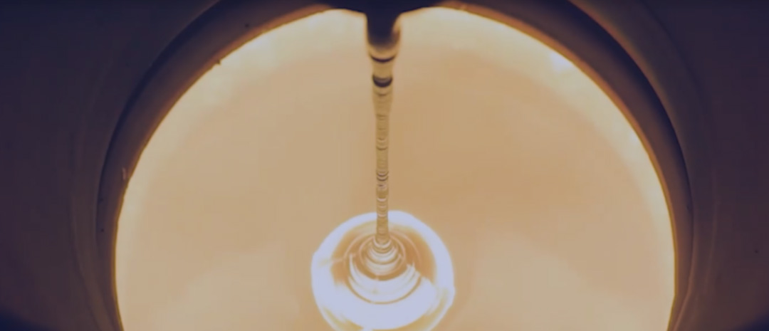
3、Monocrystalline Silicon Growth There are two main methods for growing monocrystalline silicon: the Czochralski (CZ) method and the Float Zone (FZ) method. The Czochralski method is the mainstream technology, where polycrystalline silicon is placed in a crucible and heated to a molten state. A seed crystal is then brought into contact with the molten silicon and slowly pulled upward to form monocrystalline silicon. The Float Zone method involves heating a polycrystalline silicon rod in a vacuum or inert gas environment with an electric field, causing localized melting. By moving the heating zone and slowly pulling the seed crystal, a high-resistivity, high-purity monocrystalline silicon rod is formed.
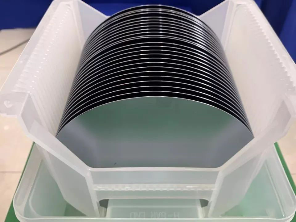
4、Silicon Ingot Processing The grown monocrystalline silicon ingot needs to be ground to achieve a standard diameter and then sliced into thin wafers. The edges of the sliced wafers are sharp and need to be beveled to create smooth edges.
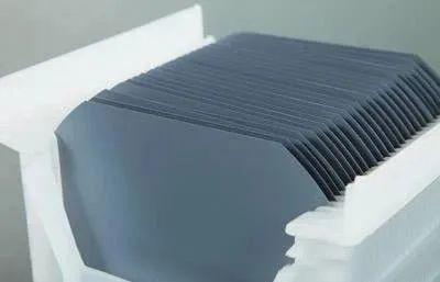
5、Silicon Wafer Polishing The polishing process aims to make the surface of the silicon wafer smoother, free of damage, and ensure thickness consistency. This step is crucial for the subsequent chip manufacturing.
6、Testing and Packaging The polished silicon wafers undergo electrical property testing, such as resistivity testing. Depending on the requirements, the wafers may undergo epitaxial growth to form epitaxial silicon wafers with specific electrical properties.
Building 1, Lian Dong U Valley, Shenzhen Road, Feixi County, Hefei City, Anhui Province, China
Friendly Links :
© 2025 United Energy Co.,ltd All Rights Reserved.